Lab note: CMOS analog switch non linearity
CMOS analog switches are a very convenient way to pass signals around: they work up to MHz frequencies, they don't statically consume power and their two terminals can float arbitrarily between the rails. Their downsides are their badly characterized ON resistance, and the fact that it varies with applied voltage...
This has made them shunned in some audio circles, because this brings distortion. But I grabbed a whole bag of DG212CJ quad analog switches at 39C3, and it'd be a shame not to use them.
Getting to know our chip
The switch has 4 supply pins: for the analog parts, then and GND for logic biasing. Each section has a TTL-compatible enable pin, which turns on or off the analog switch between the D and S pins. Here D and S are interchangeable, since the substrate of the two transistors is not biased from them.
Here's the relevant excerpt from the Intersil datasheet; they named D and S as IN and OUT. I think the transistors at the center are there to provide proper OFF behavior under various conditions.
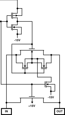 The switch itself is made from two large MOSFETs wired in parallel;
one of them is P-type and the other is N-type. When the switch
is ON, both are turned on. They both operate in their "triode",
or resistive, region. The resistance is around 100 to 200Ω.
As S and D approach the positive supply, the bias on the N-type
transistor becomes weaker, and it eventually turns off.
This increases the effective resistance, because only the P-type
will then conduct. The reverse happens when S and D get too close
to the negative rail: the P-type shuts off and the whole current
is conducted by the N-type.
The switch itself is made from two large MOSFETs wired in parallel;
one of them is P-type and the other is N-type. When the switch
is ON, both are turned on. They both operate in their "triode",
or resistive, region. The resistance is around 100 to 200Ω.
As S and D approach the positive supply, the bias on the N-type
transistor becomes weaker, and it eventually turns off.
This increases the effective resistance, because only the P-type
will then conduct. The reverse happens when S and D get too close
to the negative rail: the P-type shuts off and the whole current
is conducted by the N-type.
This is the first cause of non linearity: clearly, the effective resistance varies depending on (say) . There is another cause of non linearity; if is fixed, and allowed to vary a lot, the transistors get closer to saturation. This decreases their effective conductance, rising the overall resistance.
Near zero current, we can linearize with respect to and say that:
What's of interest to me is the behavior of the above near and with . The typical application is one where the switch connects an audio source to a relatively high impedance load, say . You can think how that would model an opamp amplifier connected to the signal, for instance. The strongest audio "line-level" signals one would want to process have amplitude = 2.5V at most.
We want to know the effect of those two components.
I did some rough order-of-magnitude calculations for the second one. The MOSFET state equations give that in a transistor, the relative resistance deviation due to a (small) is given by where is the bias voltage turning the transistor on. Near , the bias voltage is going to be around 12V for each transistor, is going to be a few hundred microamps () such that will be about ten millivolts or so. We thus expect the resistance deviations to be on the order of . The overall gain deviation in the suggested application would be roughly (recall ), which computes out to gain error. In audio terms, that's a distortion about 100dB weaker than the signal. As we'll see, this is completely negligible compared to the variations of with .
As long as we measure with sufficiently low , we can model
Reading through the previous estimations, we see that we'd like to measure resistance slopes of around 1 or .1 Ω/V. Anything lower is inconsequential.
Measurements
I quickly set-up the following test circuit on a breadboard:
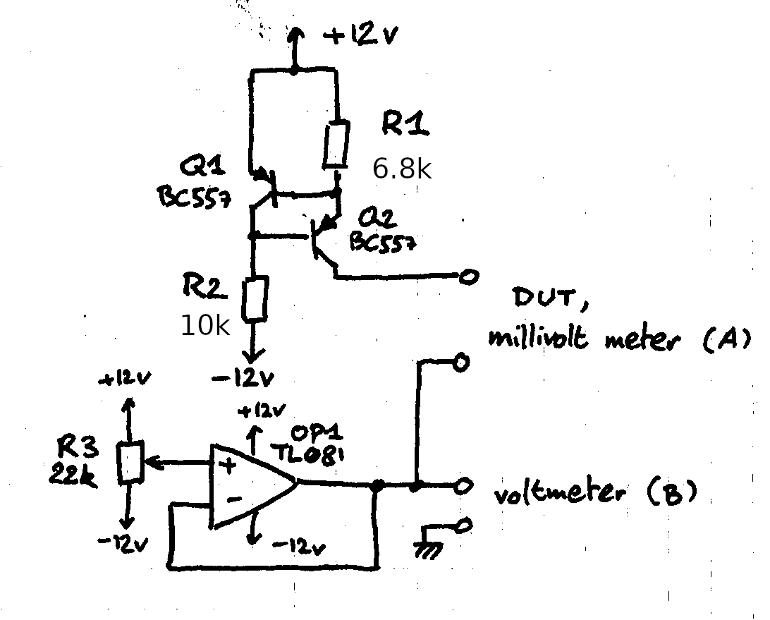 Transistors Q1 and Q2 make a constant current source, the opamp sets . Nothing too fancy.
Three things were connected to the DUT pins:
- First, they were shorted, just to test that multimeter A's millivolt scale had a decent zero.
- Secondly, I did a calibration run with a 1kΩ resistor; the voltage should be
constant and that gives us the overall gain of the setup.
- Finally, I measured a turned-on DG212.
In each run, the potentiometer is adjusted to sample at various values.
Transistors Q1 and Q2 make a constant current source, the opamp sets . Nothing too fancy.
Three things were connected to the DUT pins:
- First, they were shorted, just to test that multimeter A's millivolt scale had a decent zero.
- Secondly, I did a calibration run with a 1kΩ resistor; the voltage should be
constant and that gives us the overall gain of the setup.
- Finally, I measured a turned-on DG212.
In each run, the potentiometer is adjusted to sample at various values.
The first run reported a straight 0.0mV for each measurement -- it seems we're clear here.
The calibration run showed the gain to be steady with respects to , which was the main concern.
A previous attempt at this setup with an LM317 for the current source failed miserably at this
step. I had forgotten it needed a minimum current of 10mA to maintain regulation... far above
the 100µA of this setup. The last run yielded the following plot:
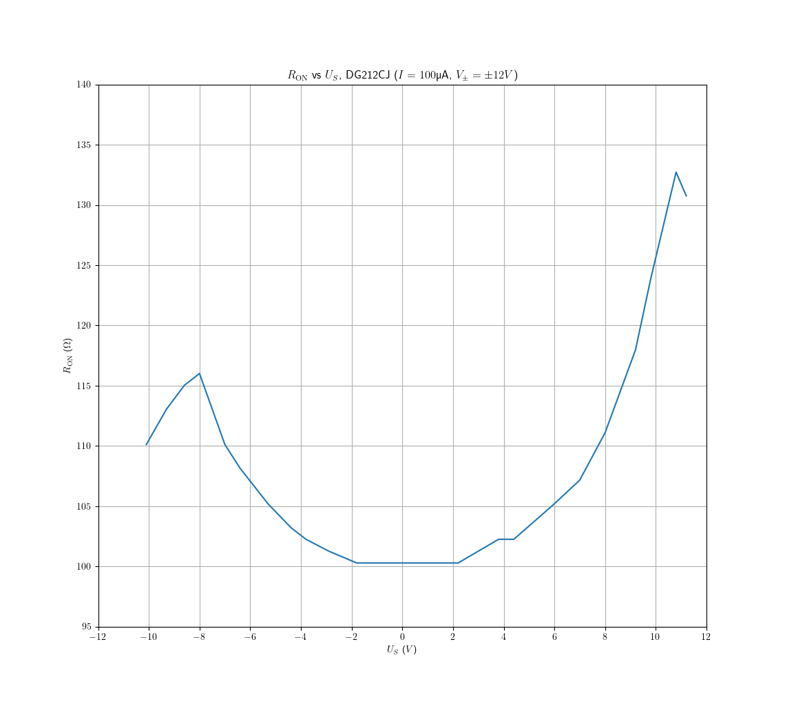 This is exactly the curve we expected. The resistance is approximately constant near zero,
then there are two bumps as the signal gets closer to the rails. (I haven't been able to find
a good explanation of why the resistance goes down very near the rails -- intrinsic diode biasing
maybe? It's a common feature of such plots.) The bump with is larger than the other one;
that's because the P-type transistor is weaker than the N-type, so its resistance is greater.
It seems I had a particularly good sample here, the datasheet lists the typical ON resistance as
150Ω but I only had 100 here.
This is exactly the curve we expected. The resistance is approximately constant near zero,
then there are two bumps as the signal gets closer to the rails. (I haven't been able to find
a good explanation of why the resistance goes down very near the rails -- intrinsic diode biasing
maybe? It's a common feature of such plots.) The bump with is larger than the other one;
that's because the P-type transistor is weaker than the N-type, so its resistance is greater.
It seems I had a particularly good sample here, the datasheet lists the typical ON resistance as
150Ω but I only had 100 here.
Clearly, past ±3V the non linearity is appreciable, and our measurement resolves it nicely. The flat spot near 0V is caused by the limited resolution (100µV) of the multimeter, which quantizes the measured resistance to around 1Ω. The signals we're measuring are on the scale of 10mV, since the total resistance is around 100Ω.
I considered two options. The first one would be to add an amplifier in front of the multimeter, say with gain 10. Then, it's up to the multimeter to resolve .1mV differentials riding on a total signal of 100mV... I'm not sure I trust my multimeter to have such dynamic range, though this might've worked just fine. The other one is more fun: consider a small AC signal riding on . Then
By measuring the AC signal, we get a direct estimate of the derivative of ! The effect size
is very small, so we still need an amplifier. I set up the following circuit to test this.
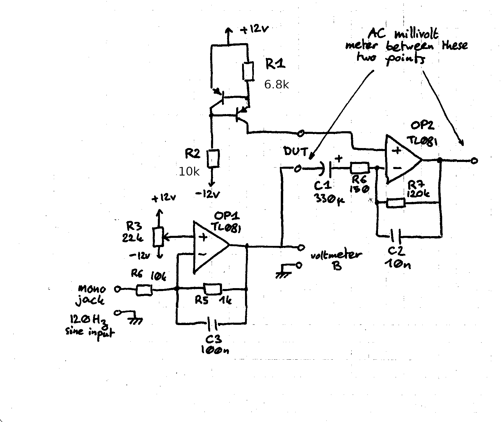 This is sloppy -- the RC time constant of the amplifier opamp is tuned to minimize noise as
much as possible, even though this reduces signal gain somewhat. Also, the common-mode rejection ratio
of the opamp is no longer negligible. A better way to do this would've been to condition the signal
further so that it could be fed back to the computer, allowing for proper lock-in detection.
This is sloppy -- the RC time constant of the amplifier opamp is tuned to minimize noise as
much as possible, even though this reduces signal gain somewhat. Also, the common-mode rejection ratio
of the opamp is no longer negligible. A better way to do this would've been to condition the signal
further so that it could be fed back to the computer, allowing for proper lock-in detection.
Anyway, here's the measurements; the orange dots are the calibration run (where DUT is a short),
and the blue dots are the measurement run. Lines represent fits.
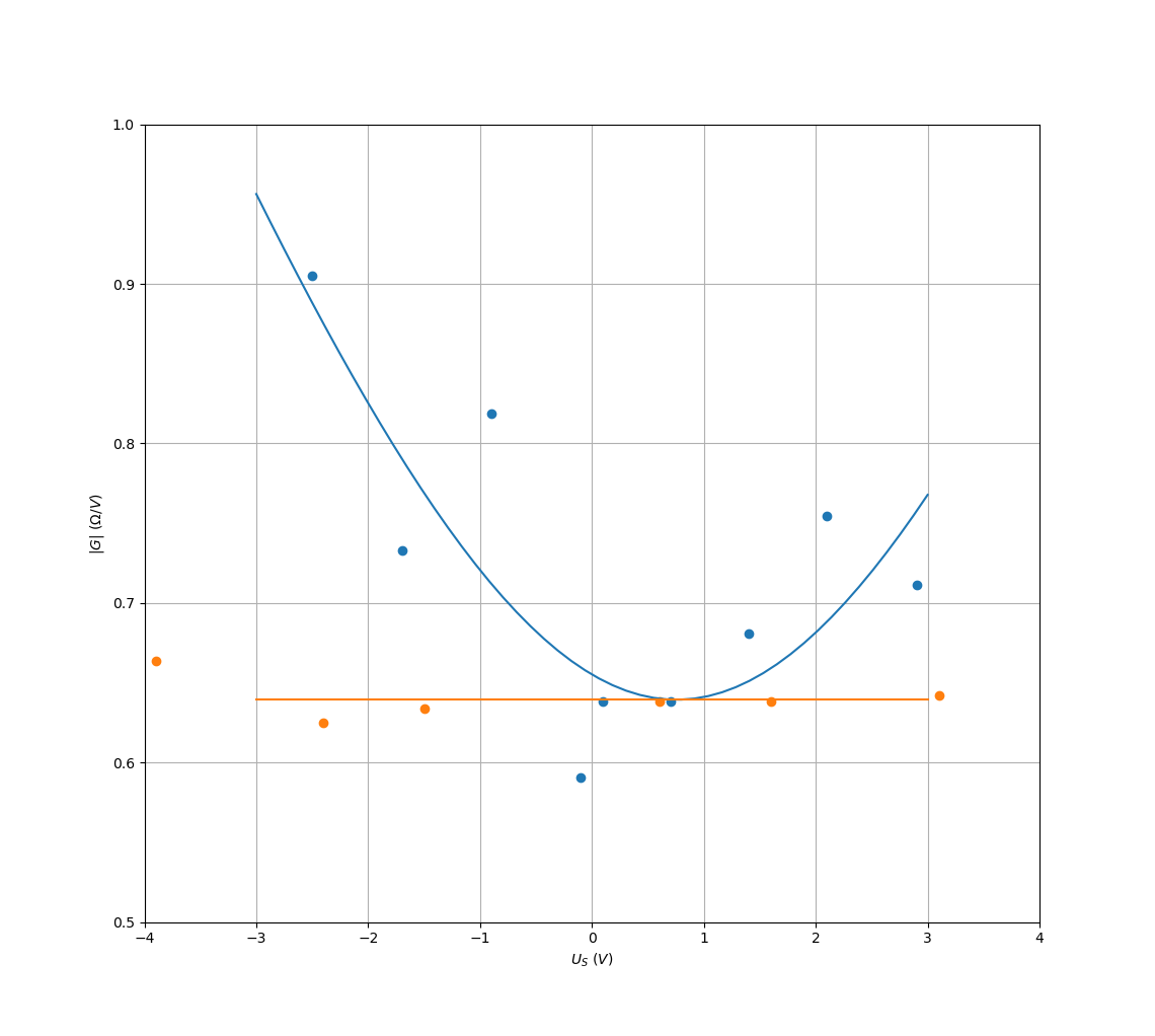 The main contribution to the zero level is the noise, and not the opamp's CMRR. But anyway, from
this shameful fit we can still extract an estimate for on
the audio range... It turns out to be .2Ω/V (I'm not giving any more significant
digits, the precision is already lower than 10%.) Assuming that a parabola is a good fit for
the inside of the bathtub curve, this gives a distortion level of around -86dB relative to the
signal. Let's be generous and round this to -80dB.
The main contribution to the zero level is the noise, and not the opamp's CMRR. But anyway, from
this shameful fit we can still extract an estimate for on
the audio range... It turns out to be .2Ω/V (I'm not giving any more significant
digits, the precision is already lower than 10%.) Assuming that a parabola is a good fit for
the inside of the bathtub curve, this gives a distortion level of around -86dB relative to the
signal. Let's be generous and round this to -80dB.
Conclusions
The goal of getting scales on analog switch distortion was achieved. For audio applications, the distortion level should be -80dB in a 10kΩ. load. This level is not suitable for studio recording environments, but in practice should be more than fine in most applications. This distortion level, with an almost-clipping input, is comparable to the noise floor I found in laptop sound card noise measurements. So I'm not going to have second thoughts using those switches in my projects.
Also, it might be a good idea to implement a proper audio vector analyzer in software, that would've been very useful. Knowing the actual accuracy of my multimeter (and, in general, of HackENS' instruments) would've been valuable too. It's not often that you want .01% accuracy, but when you do it's nice to have.